(Sample) 3rd order Multiple Feedback High-pass Filter Design Tool - Result -
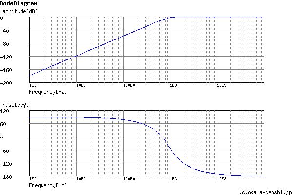
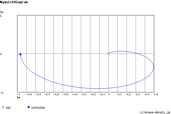
Calculated the Transfer Function for the 3rd order Multiple Feedback High-pass filter, displayed on graphs, showing Bode diagram, Nyquist diagram, Impulse response and Step response.
3rd order Multiple Feedback Filter
| Vi→ |
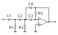
|
→Vo |
| G(s)= |
-0.969618616677s3 s3+13407.3521137s2+95087603.6433s+321567817529 |
R1 = 1000Ω
R2 = 10kΩ
R3 = 91kΩ
C1 = 0.15uF
C2 = 0.0047uF
C3 = 0.0047uF
C4 = 0.0047uF
Equivalent block diagram:
| Vi(s)→ | s s+2πfc1 | → | s2 s2+2ζ(2πfc2)s+(2πfc2)2 | →Vo(s) |
Cut-off frequency fc1, fc2 of equivalent block diagram:
fc1 = 1018.68878553[Hz]
fc2 = 1128.09512887[Hz]
Damping ratio ζ of equivalent block diagram:fc2 = 1128.09512887[Hz]
ζ = 0.494265753214
Pole(s)
p = -557.578788569 +980.665342673i[Hz]
|p|= 1128.09512887[Hz]
p = -1018.68878553[Hz]
|p|= 1018.68878553[Hz]
p = -557.578788569-980.665342673i[Hz]
|p|= 1128.09512887[Hz]
|p|= 1128.09512887[Hz]
p = -1018.68878553[Hz]
|p|= 1018.68878553[Hz]
p = -557.578788569-980.665342673i[Hz]
|p|= 1128.09512887[Hz]
Zero(s)
z = 0[Hz]
|z|= 0[Hz]
z = -0[Hz]
|z|= 0[Hz]
z = -0[Hz]
|z|= 0[Hz]
|z|= 0[Hz]
z = -0[Hz]
|z|= 0[Hz]
z = -0[Hz]
|z|= 0[Hz]
Phase margin
pm= NAN[deg] (f =0[Hz])
Oscillation frequency
f = 980.665342673[Hz]
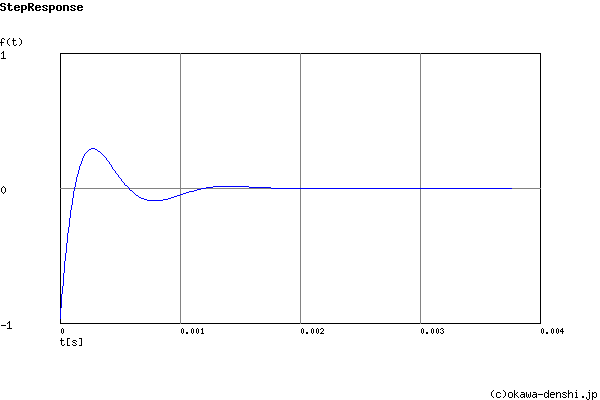
Overshoot (in absolute value)
The 1st peak gpk = 0.31 (t =0.00024[sec])
The 2nd peak gpk = -0.098 (t =0.00068[sec])
The 3rd peak gpk = 0.014 (t =0.0012[sec])
The 2nd peak gpk = -0.098 (t =0.00068[sec])
The 3rd peak gpk = 0.014 (t =0.0012[sec])
Final value of the step response (on the condition that the system converged when t goes to infinity)
g(∞) = 0
Filter gain at f=∞
k = -0.969618616677Times
Frequency analysis
Transient analysis