(Sample)Twin-T Notch Filter Design Tool - Result -
Calculated the transfer function for the Twin-T notch filter, displayed on graphs, showing Bode diagram, Nyquist diagram, Impulse response and Step response.
| Vin(s)→ |
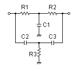
|
→Vout(s) |
| G(s)= |
s3+9090.90909091s2+41322314.0496s+368949232586 s3+36038.961039s2+284828807.556s+368949232586 |
R1 = 22kΩ
R2 = 22kΩ
R3 = 5.6kΩ
C1 = 0.01uF
C2 = 0.01uF
C3 = 0.01uF
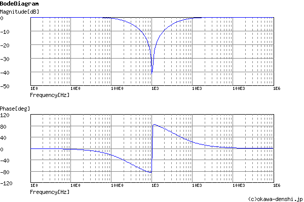
Center rejection frequency
f0 = 1023.08672291[Hz]
f0 = 1013.91087188[Hz]
f0 = 1013.91087188[Hz]
Pole(s)
p = -255.895392582[Hz]
|p|= 255.895392582[Hz]
p = -4041.77097335[Hz]
|p|= 4041.77097335[Hz]
p = -1438.11242732[Hz]
|p|= 1438.11242732[Hz]
|p|= 255.895392582[Hz]
p = -4041.77097335[Hz]
|p|= 4041.77097335[Hz]
p = -1438.11242732[Hz]
|p|= 1438.11242732[Hz]
Zero(s)
z = -4.34076355049 +1016.95722029i[Hz]
|z|= 1016.96648427[Hz]
z = -1438.18159192[Hz]
|z|= 1438.18159192[Hz]
z = -4.34076355049-1016.95722029i[Hz]
|z|= 1016.96648427[Hz]
|z|= 1016.96648427[Hz]
z = -1438.18159192[Hz]
|z|= 1438.18159192[Hz]
z = -4.34076355049-1016.95722029i[Hz]
|z|= 1016.96648427[Hz]
Phase margin
pm= NAN[deg] (f =0[Hz])
The system does not oscillate.
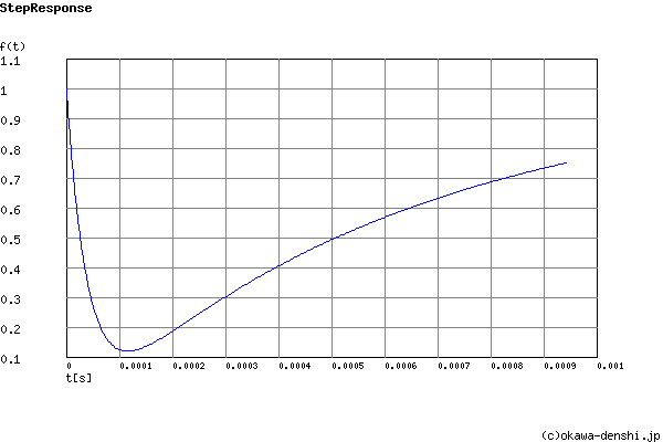
Overshoot (in absolute value)
The 1st peak gpk = 0.12 (t =0.00012[sec])
Final value of the step response (on the condition that the system converged when t goes to infinity)
g(∞) = 1
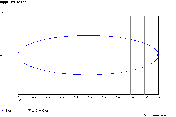
Frequency analysis
Transient analysis