(Sample)Multiple Feedback Band-pass Filter Design Tool - Result -
Calculated the Transfer Function for the multiple feedback band-pass filter, displayed on graphs, showing Bode diagram, Nyquist diagram, Impulse response and Step response.
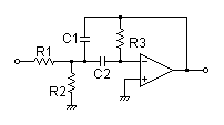
Multiple Feedback Band-pass Filter
| Vin(s)→ |
|
→Vout(s) |
| G(s)= |
-8912.65597148s s2+9238.72875092s+41335488.7073 |
R1 = 5.1kΩ
R2 = 20kΩ
R3 = 8.2kΩ
C1 = 0.022uF
C2 = 0.033uF
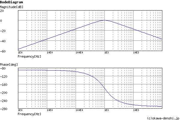
Center frequency
f0 = 1023.2498036[Hz]
Gain at center frequency f0
Gpk = -0.964705882353[times] (-0.312101466612)[dB]
Quality factor
Q = 0.695903982559
Damping ratio
ζ = 0.718489924661
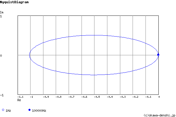
Pole(s)
p = -735.194674297 +711.70847364i[Hz]
|p|= 1023.2498036[Hz]
p = -735.194674297-711.70847364i[Hz]
|p|= 1023.2498036[Hz]
|p|= 1023.2498036[Hz]
p = -735.194674297-711.70847364i[Hz]
|p|= 1023.2498036[Hz]
Zero(s)
z = 0[Hz]
|z|= 0[Hz]
|z|= 0[Hz]
Phase margin
pm= NAN[deg] (f =0[Hz])
Oscillation frequency
f = 711.70847364[Hz]
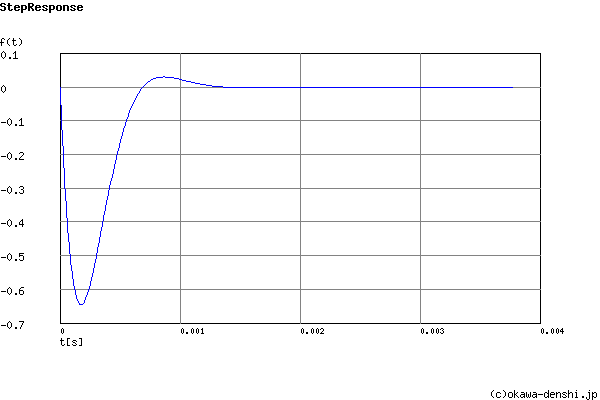
Overshoot (in absolute value)
The 1st peak gpk = -0.63 (t =0.00017[sec])
The 2nd peak gpk = 0.024 (t =0.00088[sec])
The 3rd peak gpk = -0.00095 (t =0.0016[sec])
The 2nd peak gpk = 0.024 (t =0.00088[sec])
The 3rd peak gpk = -0.00095 (t =0.0016[sec])
Final value of the step response (on the condition that the system converged when t goes to infinity)
g(∞) = 0
Frequency analysis
Transient analysis